Hiner-pack have many years of design,manufacturing experience in the field of JEDEC trays.We have produced a full range of JEDEC style trays for many customers who are specialized in semiconductor packaging and test.
Hiner- pack is committed to the development and design of the most advanced JEDEC trays,company is equipped with advanced mould processing and injection molding equipment,and a variety of testing equipment to ensure product quality, JEDEC trays designed and manufactured by Hiner- pack could provide IC and IC module with completely different electrostatic level protection and convenient transportation approaches. A number of materials can be selected to meet customer's temperature-resistant baking requirements.
Designs conforms JEDEC international standard, and has strong versatility.
Optimal product design,can provide a variety of packaging IC with protection and while reducing transportation costs.
V type tray designs, with added protection for IC substrate edge ball placement.
A variety of materials for customers to choose from to meet your ESD and process requirements.
Support for non- standard format customization.
BGA,QFN,QFP,PGA,TQFP,LQFP, SoC SiP etc. All packaging methods are available. Can be customized based on customers requirement(e.g: ESD property, Baking Temp,Baking Time).
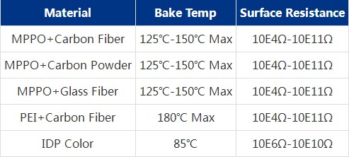
| Material |
Bake Temp |
Surface Resistance |
| MPPO+Carbon Fiber |
125℃-150℃ Max |
10E4Ω-10E11Ω |
|
| MPPO+Carbon Powder |
125℃-150℃ Max |
10E4Ω-10E11Ω |
|
| MPPO+Glass Fiber |
125℃-150℃ Max |
10E4Ω-10E11Ω |
|
| PEI+Carbon Fiber |
180℃ Max |
10E4Ω-10E11Ω |
|
| IDP Color |
85℃ |
10E6Ω-10E10Ω |