Our company's core R&D team possesses extensive experience in semiconductor handling and transport packaging solutions, with deep knowledge of industry standards and customer requirements.
From mold design, manufacturing, material development and application, to injection molding, dust-free cleaning, and quality inspection, all independently completed.
Hiner-pack has mastered key R&D capabilities and manufacturing processes, enabling maximum flexibility in customization and helping customers reduce costs.
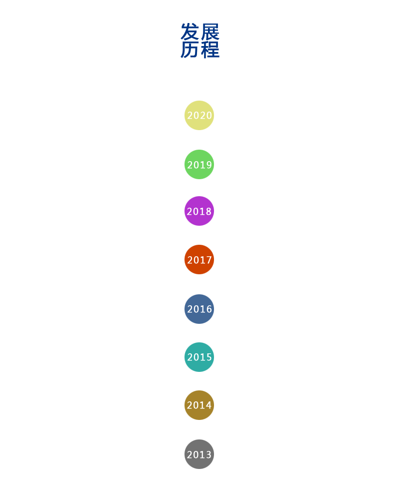
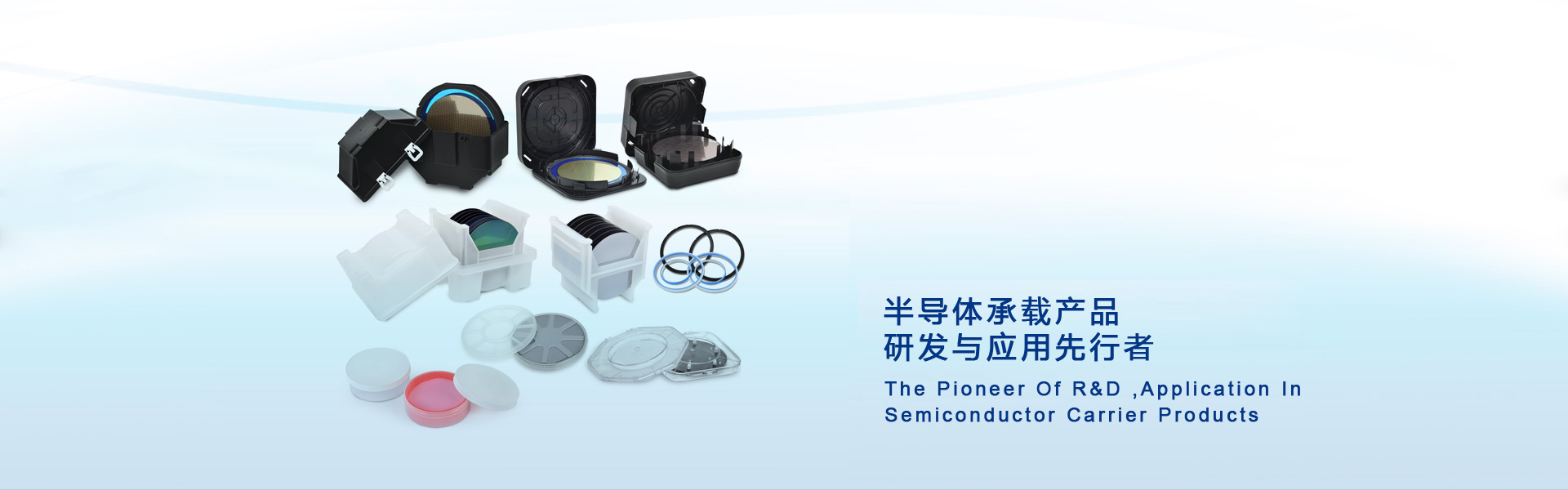
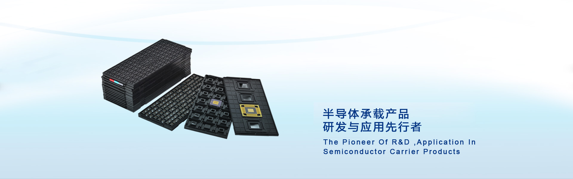
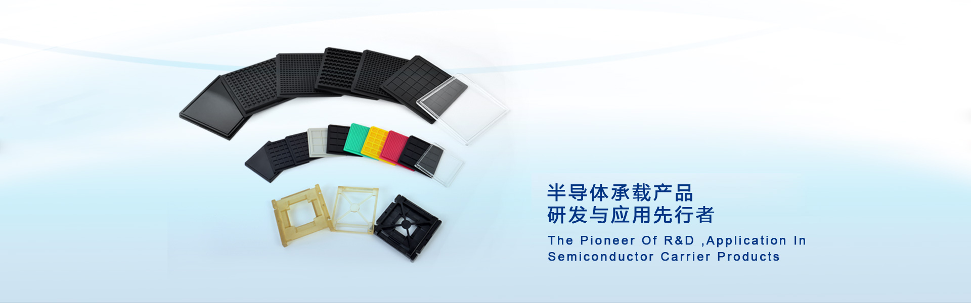
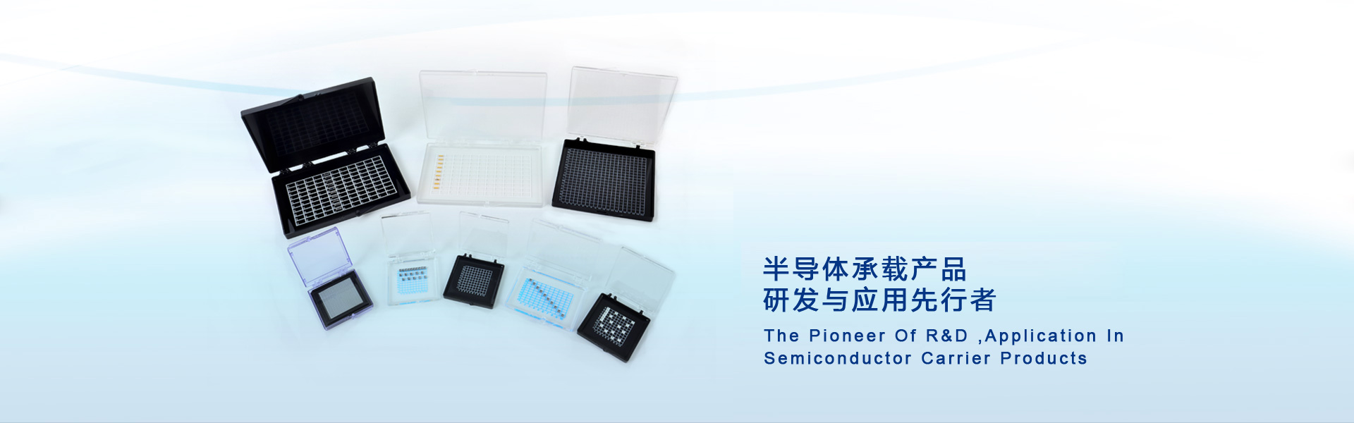
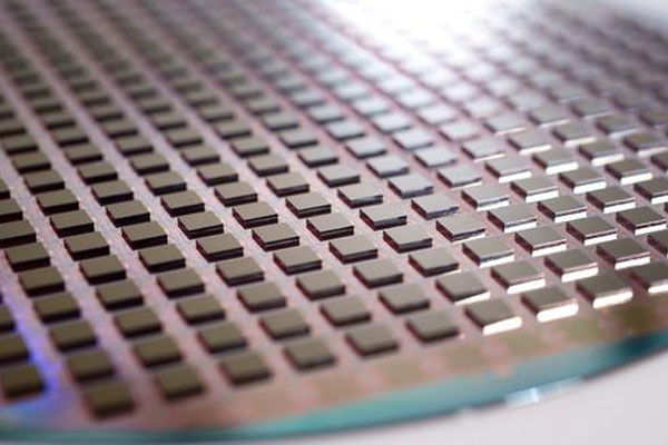
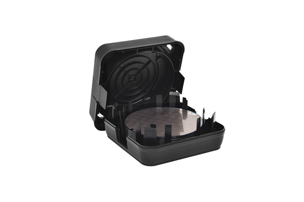
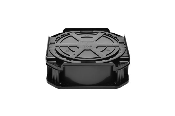
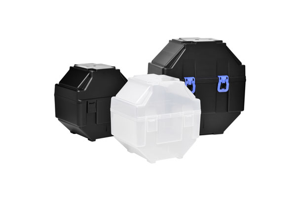
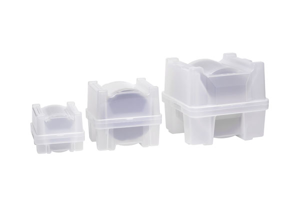
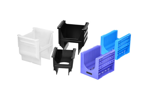
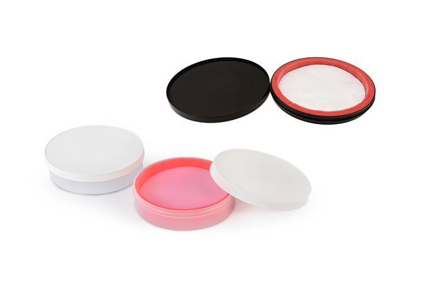
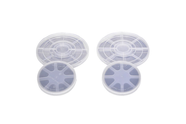
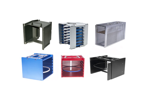
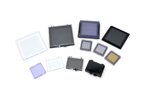
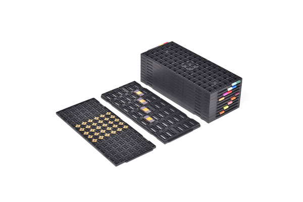
Hiner-pack® was founded in 2013. It is a comprehensive one-stop supplier integrating the design, manufacturing, and sales of automated handling, carrying, and packaging products used in semiconductor wafer fabrication and IC chip packaging and testing processes.
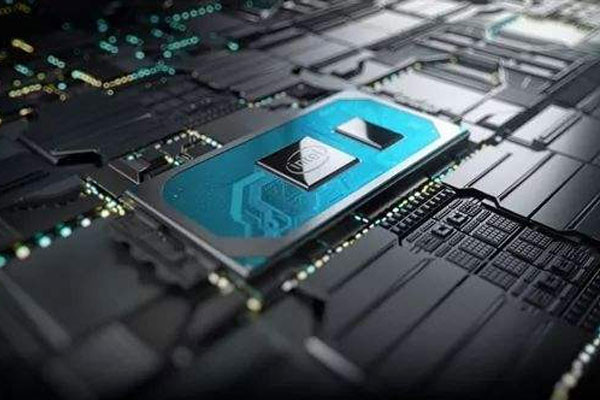
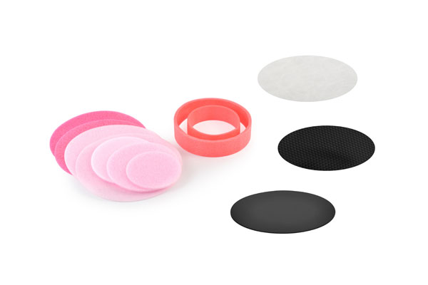
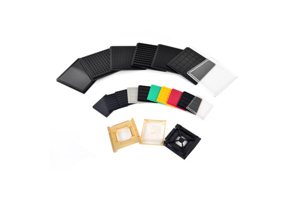
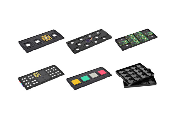
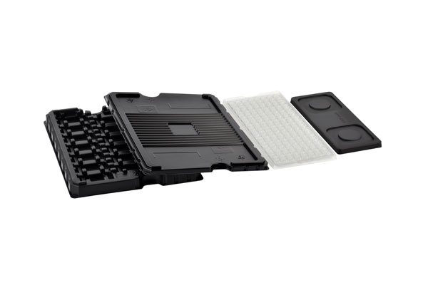
Our products are widely used in wafer fabrication and processing, IC chip packaging and testing, as well as assembly and handling of IC chip products.
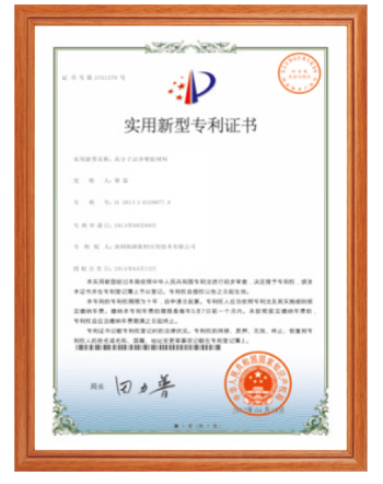
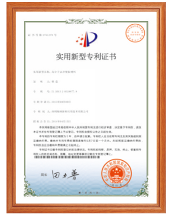
Hiner-pack is equipped with advanced mold processing and injection molding facilities, high-grade cleanroom washing lines, and a wide range of testing equipment. We have established deep cooperative relationships with many well-known enterprises, and jointly built R&D bases for polymer materials with domestic universities and research institutes. Through years of development, we have mastered specialized processing techniques and manufacturing capabilities for semiconductor packaging raw materials, and hold multiple invention and utility model patents. Thanks to our persistent efforts, we have built a professional team for material R&D and product design, continuously optimizing our semiconductor packaging solutions and launching new products to better meet customers' high standards for product quality.
Hiner-pack sincerely looks forward to providing you with high-quality service.
In order to meet the needs of the national industry planning as the main goal, to promote the development of China's semiconductor handling and packaging transport solutions as our own responsibility, and strive to become a wold-class one-stop supplier.
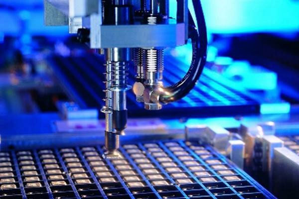
Advanced injection molding equipment / powerful mold processing ability / high-level dust-free cleaning line.
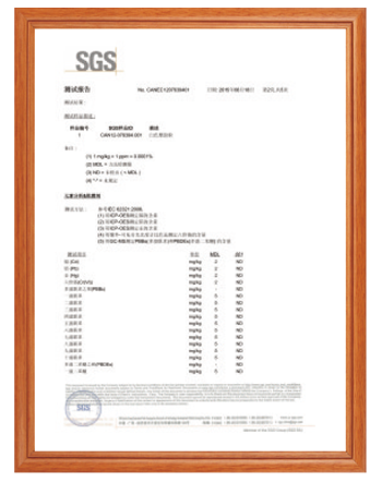
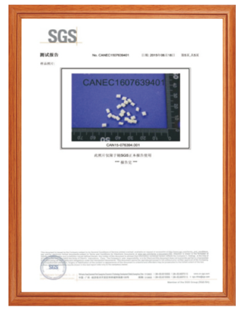
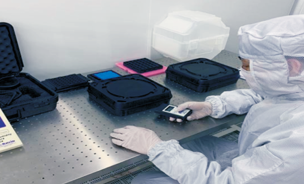
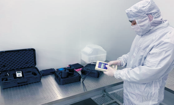
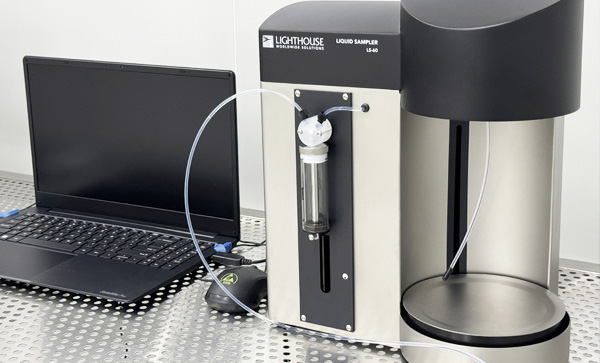
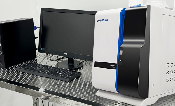
A variety of testing equipment can analyze the physical characteristics of plastic raw materials and finished products to ensure the quality.
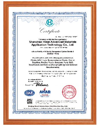
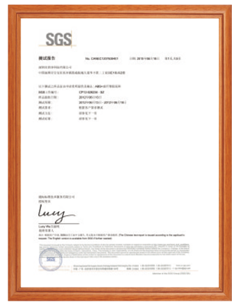
We have passed ISO9001 IATF16949 and ISO14001 certification. ensure that in the manufacturing process, from design and development, supplier selection and management, raw material inspection, manufacturing process management, reliability testing to delivery inspection, the advanced quality management system ensures to meet the quality requirements of customers.
We have established a research and Development Center for semiconductor materials with domestic universities and scientific research institutions, applied for a number of invention and utility model patents, and constantly developed new materials and products to meet customers' demands for high-quality products.

Masayoshi son, Softbank chief executive, said on Wednesday local time that Softbank goal is to control more than 90% of the chip market, according to CNBC.
Softbank acquisition of arm is just the beginning of an explosive growth in semiconductor demand, as robots will surpass humans in the fiel...
|
In order to speed up the implementation of AI applications, in addition to clear business models or application functions
In addition, the overall performance of semiconductor components also directly affects the development of AI market. Recently, in addition to more actions by silicon intelle...
|
Tsinghua Ziguang group has invested 24 billion US dollars to build the country first high-level memory chip factory in Wuhan, moving towards the goal of playing an important role in the global chip market, which has also alarmed Washington.
The Wall Street Journal analysis pointed out that the ...
|


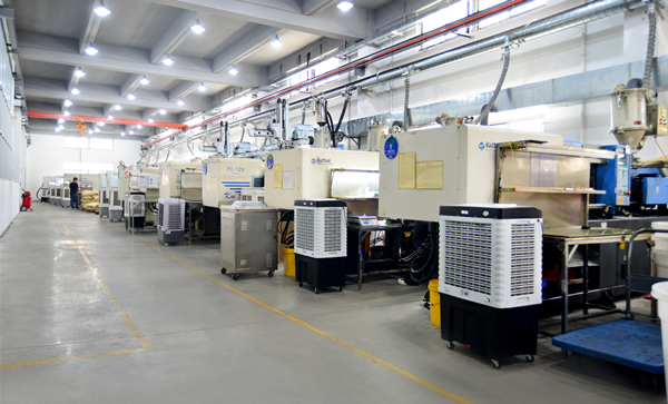 Injection Workshop
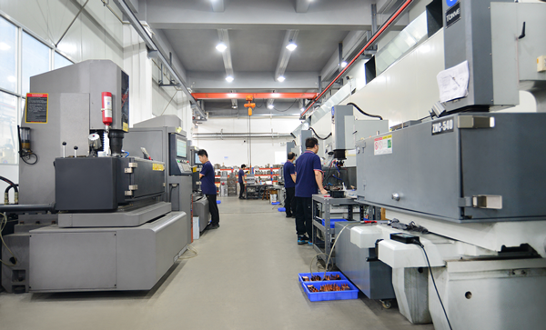 Mold Processing Workshop
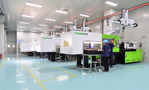 Dust Free Injection Workshop
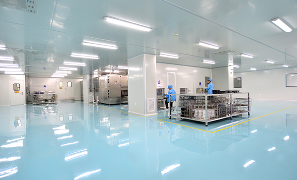 Dust Free Cleaning Workshop
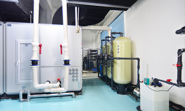 Pure Water Workshop
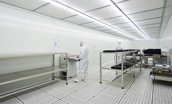 100 Class Purification Packaging
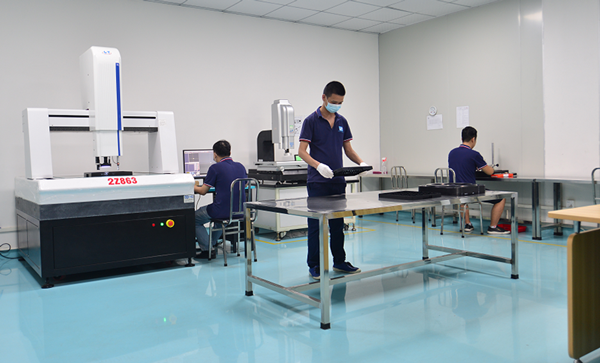 Quality Inspection Room
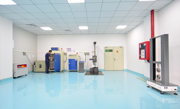 Reliability Test Room
 Static Voltage Tester
 Precision Resistance Tester
 LPC Tester
 lonic Tester